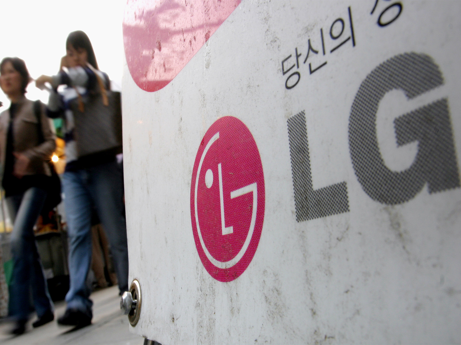
LG Electronics accelerates return to semiconductor sector
Sep 17, 2025
Seoul [South Korea], September 17 : LG Electronics is ramping up efforts to commercialise semiconductor equipment for high-bandwidth memory (HBM) as demand for chip packaging tools surges with the spread of artificial intelligence (AI), as per a report by Pulse, the English service of Maeil Business Newspaper Korea.
As per the Pulse report, the company launched the full-scale development of a hybrid bonder, which has been dubbed the "dream technology" in next-generation processes.
LG is reported to be accelerating its shift toward business-to-business (B2B)-driven "qualitative growth" while seeking synergy across its semiconductor smart factory solutions, heating, ventilation, and air conditioning (HVAC) systems, and chip equipment businesses.
Quoting industry sources, the Pulse report said LG has formed a consortium with Inha University, Gyeongbuk Technopark, and small equipment makers to carry out a national project for "HBM hybrid bonder development." The target is to complete proof-of-concept (POC) validation by 2028 and begin full-scale commercialisation by 2030.
A hybrid bonder is a semiconductor tool that directly bonds DRAM layers without bumps during the HBM stacking process, significantly improving power efficiency, wiring density, and processing speed compared with traditional thermos-compression bonders. It is considered a key enabler for next-generation HBM production, but no company has yet succeeded in mass-producing the product.
LG's entry into this field stems from a decade of semiconductor equipment research and development (R&D) led by its production technology center. The company already has experience supplying standard bonder machines that attach chips to substrates to outsourced semiconductor assembly and test (OSAT) firms, and building on this experience, it is expanding into more complex and precise semiconductor equipment. LG is also fast-tracking the development of other tools, including precision laser systems for semiconductor glass substrates and six-sided high-speed inspection machines for HBM, diversifying its equipment portfolio.
LG's entry into this field stems from a decade of semiconductor equipment research and development (R&D) led by its production technology center.
The company already has experience supplying standard bonder machines that attach chips to substrates to outsourced semiconductor assembly and test (OSAT) firms, and building on this experience, it is expanding into more complex and precise semiconductor equipment.
As per the same Pulse report, LG is also fast-tracking the development of other tools, including precision laser systems for semiconductor glass substrates and six-sided high-speed inspection machines for HBM, diversifying its equipment portfolio.
LG is notably pursuing an integrated strategy that goes beyond equipment development to encompass smart factory solutions and HVAC businesses and is aimed at the broader AI infrastructure market.
By linking semiconductor plant automation, eco-friendly HVAC systems, and next-generation bonders, the company is building a structure that covers not only equipment supply but also the entire "AI data center and semiconductor production ecosystem."
"All of this aligns with LG's emphasis on B2B-driven qualitative growth, which already accounts for about 50 per cent of sales and nearly 80 per cent of operating profit," the Pulse report read.
"The momentum comes from commitment at the top, with LG Electronics CEO Cho Joo-wan recently posting on social media that the company is "expanding its portfolio to support AI infrastructure by investing in specialized technologies essential for next-generation HBM production." Cho also told reporters on September 5th at IFA 2025 in Berlin that components and equipment are among LG's future growth pillars."
Industry observers are watching LG closely, with Hanmi Semiconductor, Netherlands-based Besi, Singapore's ASMPT, and Hanwha Semitech among the global companies that developing hybrid bonding technologies. If LG secures mass production capability, analysts say it will significantly boost the competitiveness of Korea's semiconductor equipment ecosystem.
The market outlook is favorable. According to Business Research Insights, the global hybrid bonding market is projected to grow from USD 199 million this year to USD 713 million by 2034 at an annual growth rate above 15 per cent.