3D Glass Solutions to invest Rs 1,943 crore in Odisha for advanced chip packaging facility; Targets 2030 production
Apr 19, 2026
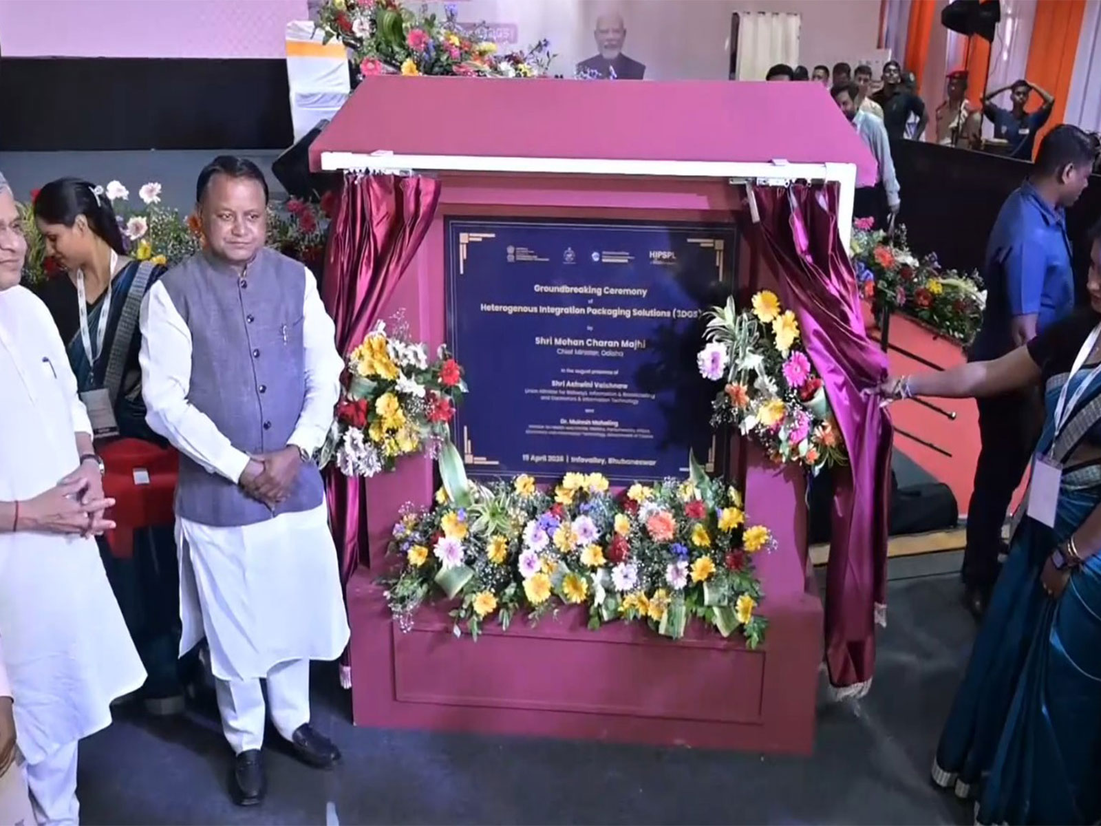
Khordha (Odisha) [India], April 19 : US-based 3D Glass Solutions (3DGS), through its wholly owned Indian subsidiary Heterogenous Integration Packaging Solutions Pvt Ltd (HIPSPL), is implementing a greenfield, vertically integrated advanced packaging and embedded glass substrate ATMP facility at Info Valley, Khordha district in Odisha.
The project entails a total investment of Rs 1,943.53 crore, including eligible capex of Rs 1,598.33 crore. Approved central fiscal support amounts to Rs 799 crore, with additional state support of Rs 399.5 crore. The project is being funded through equity (Rs 745 crore), government support, with no external debt envisaged at this stage.
3DGS brings proprietary glass-ceramic packaging technology based on its APEX platform, with over 100 patents and 31 active patent families covering materials, manufacturing processes, device design, and system-level integration.
The technology offers advantages such as a lower dielectric constant (3-6 vs 11.7 for silicon), improved signal integrity at high frequencies (1-200 GHz), better thermal stability, and reduced transmission losses. The company currently operates a facility in Albuquerque, New Mexico, producing glass-based devices including high-value 3DHI modules for aerospace applications.
The product portfolio includes glass FCBGA substrates and packages, RF and AiP SiP modules, glass interposers with embedded passives and silicon bridges, and 3DHI modules. These products are targeted toward high-growth application areas such as data centres, high-performance computing (HPC), AI, machine learning, 5G/6G communication systems, photonics, automotive radar, and defence electronics.
The facility is designed as a vertically integrated operation combining substrate manufacturing, assembly and advanced packaging within a single site, which is distinct from conventional OSAT models. The project comprises three key manufacturing segments.
The first segment is the glass panel processing (510 mm x 515 mm), unit with an installed capacity of 5800 panels/month. This unit will manufacture embedded glass substrates and interposers using panel-level processing technology representing a transition from the company's existing 150 mm and 200 mm wafer-based processes deployed in its Albuquerque facility. The panel-based approach is expected to enable higher throughput and cost efficiencies but remains an emerging technology globally.
The second segment is the assembly and packaging unit with an initial capacity of approximately 4.2 Mn units/month. This unit will produce advanced packages including Glass FCBGA, RF SiP, and AiP modules. The assembly line is designed to process both internally manufactured glass substrates and externally sourced organic substrates in the initial phase, with a gradual transition toward glass-based packaging as ecosystem maturity improves.
The third segment is the 3DHI module unit, with a capacity of 13,330 modules per year. This unit focuses on high-value, low-volume applications involving stacking of multiple glass layers with integrated semiconductor dies (CMOS, GaN, RF components, passives), targeting aerospace, defence, and high-frequency communication systems. These modules are characterized by high complexity and significantly higher realization per unit.
As of April 2026, site-related activities including soil testing and preliminary engineering have been completed, and applications for environmental clearance, SEZ and building permits are in progress. Engineering design and EPC planning are being undertaken in collaboration with Tata Consulting. Equipment vendor discussions are ongoing, including identification of toolsets required for panel-level processing. Commercial production is expected to commence by August 2028, with volume production targeted by August 2030.
The project has demonstrated strong market traction, with LoI received from multiple global customers. Indicative commitments include approximately 70,000 panels/year from Marvell, over 10,000 panels/year from Intel, and additional demand from Applied Materials, Xscape Photonics, AAYUNA Inc., and Xpeedic. Aggregate offtake indications exceed 100 per cent of proposed installed capacity, providing strong demand visibility.
Strategically, the project is positioned to introduce glass substrate-based advanced packaging capabilities in India, a segment currently dominated by a limited number of global players. It aligns with emerging trends in heterogeneous integration, chiplet architectures, and high-density interconnects required for next-generation computing systems. The project is also expected to support domestic requirements in strategic sectors such as defence, space, and telecommunications.