Semicon 2026 Day 1: Rs 1 lakh crore investment commitments, 16 MoUs and announcements push India semiconductor ecosystem deeper
Sep 17, 2026
New Delhi [India], September 17 : The first day of SEMICON India 2026 saw the government lay out a wider roadmap for the next phase of India's semiconductor programme, with around Rs 1 lakh crore in investment commitments, plans to create close to one lakh jobs and a series of agreements spanning chip manufacturing, materials, packaging, design and talent development.
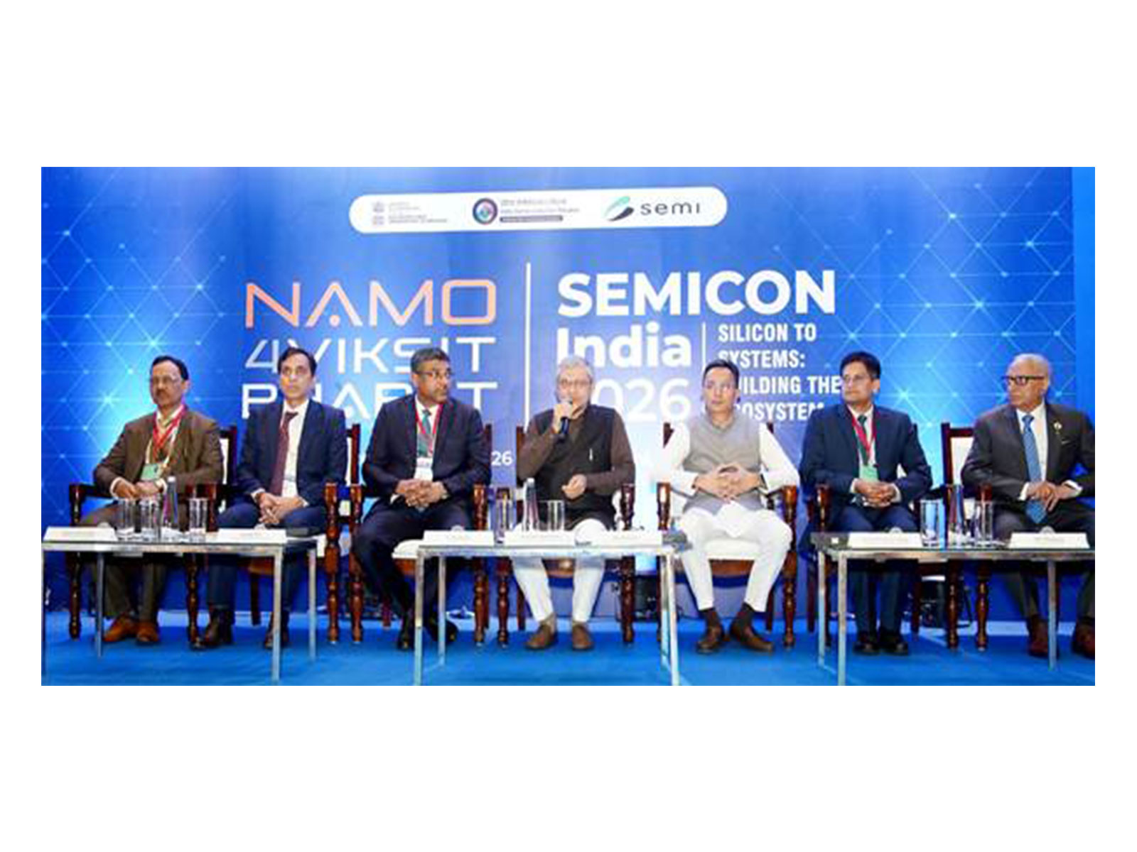
Union Electronics and Information Technology Minister Ashwini Vaishnaw outlined the implementation approach for Semicon 2.0, which will move beyond the initial focus on establishing semiconductor manufacturing facilities and seek to develop the wider ecosystem around them.
According to the Ministry of Electronics and Information Technology, Semicon 2.0 is aimed at "putting the wider ecosystem in place" and scaling capabilities across the semiconductor value chain.
Investment commitments of around Rs 1 lakh crore, or approximately USD 11-12 billion, have already been received across the Semicon 2.0 ecosystem. These investments are expected to materialise over the next two to three years as companies secure their respective board and shareholder approvals.
The proposed investments are expected to create close to one lakh new employment opportunities across the semiconductor ecosystem.
The government's next phase will be built around six broad areas - semiconductor design, machines and materials, fabrication facilities, advanced packaging, applied research and development, and talent development.
Under the design pillar, the government plans to expand support for semiconductor design start-ups and larger companies, including access to funding, venture capital and customers, along with stronger intellectual property protection.
The government is targeting 200 semiconductor design start-ups under the expanded programme. Of the 105 start-ups supported during the first phase, 20 have already secured venture capital funding.
The focus will also expand from individual chip design towards systems design, allowing Indian companies and engineers to work on more complex technology requirements.
Semicon 2.0 will also seek to build a domestic ecosystem for semiconductor manufacturing machines, equipment and materials. The government is looking to use India's existing engineering and design capabilities to attract global semiconductor equipment companies for both design and manufacturing operations.
Precision manufacturing will be another important component, with the ecosystem expected to serve semiconductor manufacturing alongside sectors such as aerospace, aviation and advanced electronics.
Expansion of fabrication capacity will cover different technologies, including display, memory, silicon, compound and logic fabs, as the government looks to widen the country's semiconductor manufacturing base.
Advanced packaging, which plays a growing role in improving chip efficiency and system-level performance, has also been identified as a separate focus area under the programme.
Research and development will see greater participation from industry, with companies encouraged to propose applied R&D projects involving the government and academic institutions. Funding for such projects will be shared between industry and the government, with a focus on technologies that can be translated into practical outcomes.
Talent development formed another major part of the Day 1 roadmap.
Around 400 universities and institutions are already engaged in semiconductor chip-design education under the first phase. The government now plans to upgrade the curriculum to help students move from foundational chip-design capabilities towards systems design.
Separately, one lakh technicians are proposed to be trained over five years through partnerships with industry and international institutions, including Taiwan's Industrial Technology Research Institute, or ITRI.
The government also stressed that semiconductor expansion would require building domestic capabilities in capital equipment, materials, gases, chemicals, precision manufacturing and supply chains rather than focusing only on individual fabrication plants.
The ministry said semiconductor facilities that have already entered commercial production are competing in global markets and their production capacity is being taken up by customers, while capacity at facilities currently under construction is also being created at a rapid pace.
The day also saw 11 MoUs and five other announcements across different parts of the semiconductor value chain.
Tata Electronics signed agreements covering several parts of the ecosystem. It entered an MoU with Nexperia for semiconductor wafer manufacturing, assembly and testing, technology collaboration and innovation.
The company also tied up with Ascendas First Space to develop a 363-acre vendor park in Dholera, Gujarat, aimed at supporting suppliers around its semiconductor fabrication facility.
Separate agreements with Fujifilm Corporation and JSR Corporation will focus on localisation and supply of critical semiconductor materials and advanced chemicals, while an MoU with BESI Singapore will focus on building advanced packaging capabilities in India.
Tata Electronics also entered into an MoU with Semiconductor Laboratory covering semiconductor design services, process technology, supply-chain localisation and talent development.
Kaynes Semicon signed agreements involving OptoML India, GridCrest Technologies and Sensesemi to explore advanced packaging, System-on-Module solutions, assembly and testing.
India Semiconductor Mission and Intel India launched an 'Introduction to Semiconductors' course, while Intel India and the New Age Makers' Institute of Technology signed an agreement for workforce development in artificial intelligence and semiconductor technologies.
Six ChipIN Regional Centres were also announced to widen access to chip-design capabilities across the country.
Among the production-related developments, Suchi Semicon and eInfochips exchanged their first batch of commercial devices, while commercial production of CDIL semiconductors was also announced along with an association with Japan's Shindengen Electric Manufacturing Company for package development.
SEMICON India 2026 will continue until September 19 at Yashobhoomi in New Delhi. The event has more than 600 participating companies and is expected to attract around 50,000 visitors from 52 countries, along with more than 400 executives and over 150 speakers.
The exhibition also includes country pavilions representing Japan, South Korea, Malaysia, the Netherlands, Singapore and Sweden, besides 12 state booths, a startup pavilion, an innovation showcase, a student hackathon and a workforce development pavilion.